
This is part 1 of a 3 part series that explains what’s inside a beacon. In this part we take a look at the physical beacon.
All beacons are similar inside because they are based on standard circuit designs from Nordic Semiconductor, Dialog Semiconductor or Texas Instruments. These semiconductor manufacturers produce a complete system on a chip (SoC) that requires minimal external components. The SoC is a small computer with memory that runs software created by the manufacturer of the beacon. We will take a deeper look at the SoC in part 2 and the software in part 3.
For this series of articles we going to take a deeper look at Minew’s i7 beacon. It’s based on Nordic Semiconductor’s nRF52832 SoC.
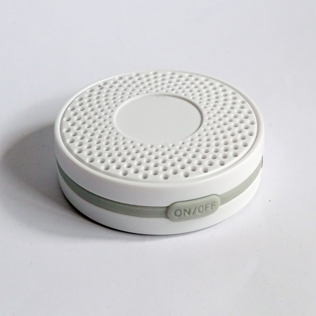
Inside the case is a PCB with a CR2477 slide in battery at the rear.
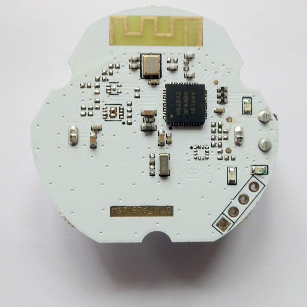
The main chip you can see is the mRF52832. At the top you can also see the antenna that’s created using a track in the printed circuit board. The holes at the bottom right are connections used to program the beacon.
To understand more, we need to look at the printed circuit board design and circuit schematic:
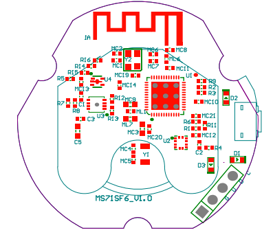
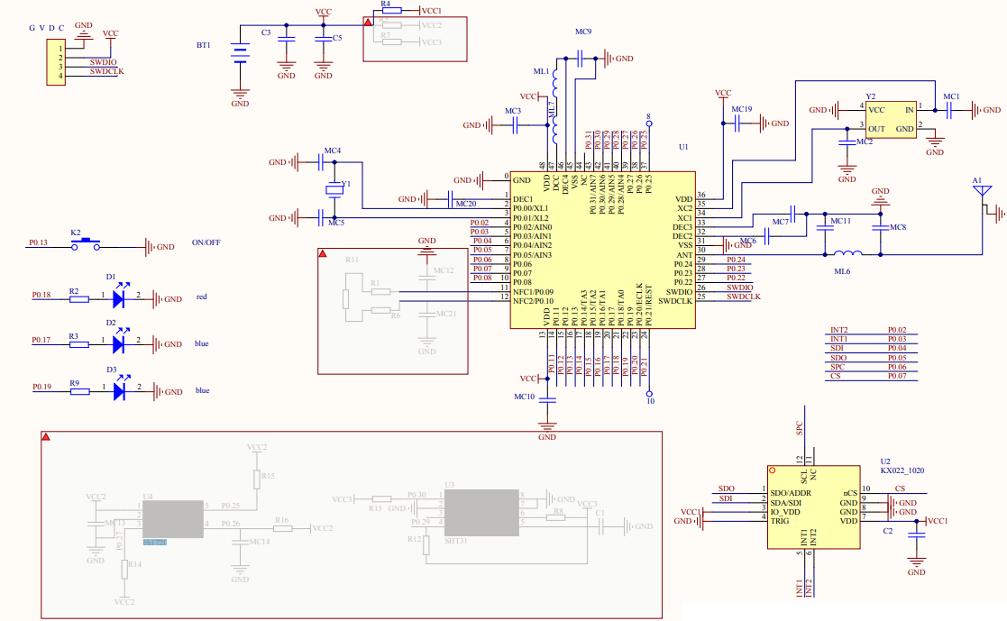
It can be seen that there aren’t many external components. Y1, the metal component at the top is the crystal used to maintain timing. The SoC has a number of programmable input/output (PIO) pins that are multi-purpose. In a beacon some are usually connected to LEDs and a switch as shown at the left hand side of the circuit diagram. There are also capacitors that need to be external to the SoC.
U2, U3 and U4 are optional for this beacon and missing from this variant of the i7. U2 is the KX022-1020 accelerometer. U3 is the SHT31 temperature/humidity sensor. U4 is the BH1721 light sensor.
In part 2 we take a closer look at the nRF52 SoC.